Consequently, the potential of each element on the
beam side approaches the potential of the signal
electrode side. It will reach a value that varies with
the amount of light falling on the element. On the
next scan, the electron stream replaces a number of
electrons on each element, just sufficient to return it
to the potential of the cathode. Because each
element is effectively a small capacitor, a capacitive
current is produced in the signal electrode circuit
that corresponds to the electrons deposited as the
element is scanned. When these electrons flow
through the load resistor in the signal electrode
circuit, a voltage, which becomes the video signal,
is produced.
PLUMBICON.— The plumbicon is similar in
appearance and operation to the vidicon.
It has
several advantages over the vidicon.
The
plumbicon has a more rapid response and produces
high-quality pictures at lower light levels. Because
of its small size and low power consumption, the
plumbicon is well suited for use in transistorized
TV cameras. Its simplicity and spectral response to
primary colors make it particularly useful in color
cameras.
A unique feature of the plumbicon is that its color
response can be varied by the manufacturer. It is,
therefore, available with spectral responses for each
of the primary colors. The color response of each
tube is identified by the letter R (red), G (green), or B
(blue) following the basic number. For example, a
plumbicon for a green channel may be designated
55875G.
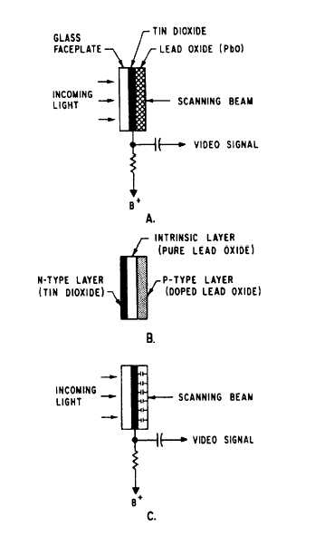
A simplified diagram of a plumbicon target is
shown in figure 5-31. The faceplate (view A) has its
inner surface coated with tin dioxide. This thin,
transparent layer is the signal plate of the target. The
tin dioxide itself is a strong N-type semiconductor.
Two layers of lead oxide are deposited on the
scanning side of the target. The first of these two is
almost pure lead oxide.
Lead oxide is an intrinsic
semiconductor. The second layer of lead oxide is
doped to form a P-type semiconductor. As shown in
view B of figure 5-31, the three layers form a P-I-N
junction.
Light from the televised scene passes through the
layer of tin dioxide and is focused on the
photoconductive lead oxide. Notice in view C of
figure 5-31 that each picture element charge acts like
a capacitor whose positive plate faces the scanning
beam. The target signal plate forms the negative
plate. As the low-velocity scanning beam strikes each
charged element, it releases electrons that neutralize
the capacitors.
SECONDARY ELECTRON CONDUCTION
(SEC).— This is a vidicon-like tube with a special
target that uses secondary electron conduction. In this
tube, light is focused on the photocathode that emits
electrons into the tube. These electrons are focused to
form an image of electron streams that strike the SEC
target. The electrons are accelerated to approximately
10,000 electron volts by the time they strike the target.
The SEC target intercepts these streams of electrons.
A great number of secondary electrons from each
Figure 5-31.-Plumbicon target.
5-25