
BASE
ZENER DIODES.--Zener diodes are special
N
P
N
diodes, commonly referred to as voltage reference
diodes. They are normally silicon rectifiers in which
EMITTER
COLLECTOR
the reverse current remains small until the breakdown
A
voltage is reached; it then increases rapidly without
further increase in voltage. Each Zener diode is
BASE
designed for a specific breakdown voltage. The
breakdown voltage varies from a few volts to several
hundred volts with different Zener diodes. A stabilized
Zener diode output (voltage or current) can be supplied
EMITTER
COLLECTOR
that is unaffected by temperature, output load, or input
voltage within given limits. The stability of the Zener
B
diode makes it very useful as a voltage reference.
ASf07007
Figure 7-7.--NPN transistor--(A) NPN diagram; (B)
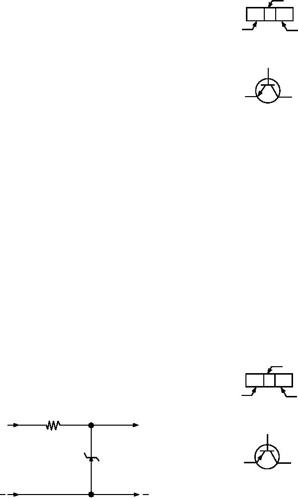
Figure 7-6 shows a basic Zener diode dc voltage
schematic symbol.
regulating circuit. A diode is selected that has a
breakdown voltage equal to the desired regulated
PNP transistors are just the opposite of NPN
output voltage. A limiting resistor is then chosen.
transistors. The N material is sandwiched between two
This resistor must drop the voltage difference
strips of P material. Figure 7-8 shows the symbol for a
PNP transistor. Notice that the emitter, base, and
current at the correct operating value. When the input
collector connections remain the same, but the arrow
voltage rises or the load current decreases, current
now points toward the base. An important point to
through the diode increases, and the voltage drop
remember on the schematic symbols for transistors is
across R1 increases so that the output voltage remains
that the arrows point toward the N material.
constant. Conversely, when the input voltage decreases
or the load current increases, the diode current
In a PNP transistor, the emitter and collector (P
decreases and the voltage drop across R1 decreases to
material) are in positive holes, and the base (N
maintain a constant output voltage.
material) has an excess of negative electrons.
A Zener diode is checked the same way a PN
How a Transistor Works.--Generally speaking,
junction diode is checked.
transistors do one of two things--they act as a
amplifier or as a switching device. Although a
TRANSISTORS.--Transistors are layers of N
transistor can either switch or amplify, normally it is
and P materials bound together. The NPN transistor is
made to do one job better than the other. For example,
prepared by placing a narrow strip of P material
amplifiers have a stable, moderate current gain (degree
between two wide strips of N material. One N section is
of amplification). Most switching applications require
called the emitter because electrons are extracted from
fast turn-on and turn-off speeds and low leakage.
the base; this section can emit electrons across the
base. The other N section is called the collector, which
BASE
is where the electrons are collected and passed down
the circuit. The base is the area electrons are drawn
P
N
P
from to permit current flow from one N section to
EMITTER
COLLECTOR
another. Figure 7-7 shows an NPN transistor and its
A
electronic symbol.
+
EIN+
E OUT
BASE
R1
CR1
EMITTER
COLLECTOR
B
ASf07008
Figure 7-8.--PNP transistor--(A) PNP diagram; (B)
ASf07006
Figure 7-6.--Zener diode voltage regulating circuit.
schematic symbol.
7-4